
SK Hynix Unveils H-TPU Controller Architecture with Over 100 Small Processors - THE ELEC, Korea Electronics Industry Media
Article excerpt
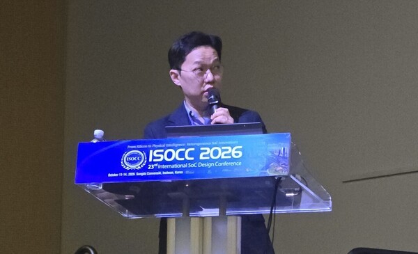
SK Hynix Inc. has disclosed the architecture and performance of its Hynix Transaction Processing Unit (H-TPU), a small processor developed in-house for solid-state drives (SSDs). The technology distributes repetitive tasks traditionally handled by general-purpose central processing units (CPUs) across more than 100 H-TPUs, significantly reducing power consumption and chip area. Koo In-je, a vice president at SK Hynix, stated at the International SoC Design Conference (ISOCC) 2026, held at Songdo Convensia in Incheon on Oct. 12, that general-purpose CPUs inside existing SSD controllers are reaching their limits in power consumption and chip area. SK Hynix developed the H-TPU to handle repetitive input/output (I/O) data-transfer paths more efficiently, he explained. The H-TPU is an ultra-lightweight programmable processor developed in-house by SK Hynix. It processes repetitive SSD operations, including read and write command processing, metadata management, and buffer control. Previously, general-purpose CPUs inside SSD controllers handled all these tasks. As SSD performance scaled up, the increasing workload required more CPU cores, which excessively expanded processor chip area and power consumption. Koo noted that Arm CPU cores commonly used in SSD controllers are overpowered for simple, repetitive tasks. These cores are optimized to process complex computations at high...
Keep reading with a free account
The rest of this article, and every signal for SK Hynix, is in your free account.
Extracted from this sentence
SK Hynix plans to apply the H-TPU technology across multiple NAND flash product lines, starting with controllers for next-generation enterprise SSDs (eSSDs).