
UC Berkeley partners with Silicon Valley facility to bring groundbreaking semiconductor research to market
Article excerpt
Highlighted: the sentence this signal was extracted from
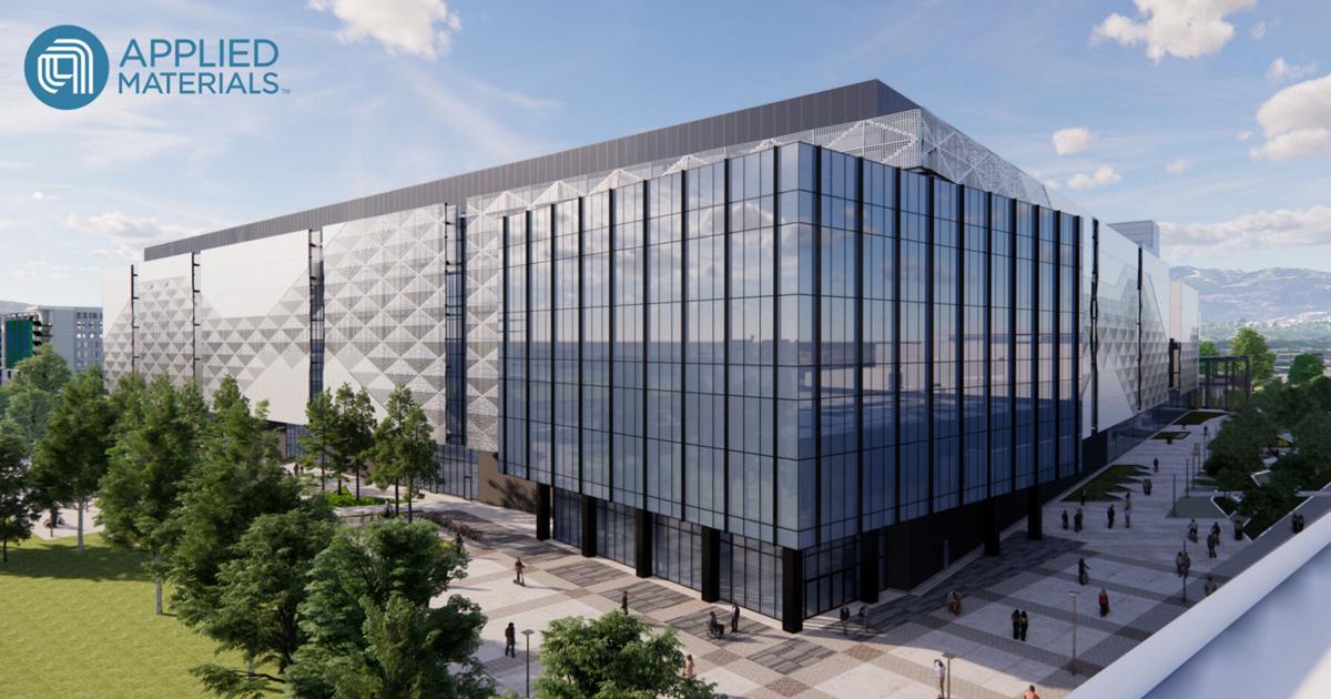
The Equipment and Process Innovation and Commercialization Center, opening in Sunnyvale later this year, is described by Applied Materials as "the world's largest and most advanced facility for collaborative semiconductor process technology and manufacturing equipment." UC Berkeley researchers will soon be able to take their semiconductor research to industry scale at a new Silicon Valley facility, helping them bring their innovations to market in the age of AI. The collaboration is a "natural evolution" of a four-decade relationship with semiconductor and display equipment company Applied Materials and may yield research funding in the future, according to an email from Julia Zolinsky, Senior Director of Development & Corporate Partnerships at UC Berkeley's College of Engineering. The facility, located in Sunnyvale, is the Equipment and Process Innovation and Commercialization Center, which Applied Materials describes as "the world's largest and most advanced facility for collaborative semiconductor process technology and manufacturing equipment (research and development)." The EPIC Center will open later this year and has also announced partnerships with Arizona State University, Rensselaer Polytechnic Institute and Stanford University. The center will also partner with major tech companies like Samsung and Taiwan Semiconductor Manufacturing Company. Semiconductors are...
Keep reading with a free account
The rest of this article, and every signal for Applied Materials, is in your free account.